Modeling the impact of incomplete conformality during atomic layer processing

We present a model for surface coverage during ALD to include precursor desorption from the surface, which leads to incomplete conformality. The model combines existing Knudsen diffusion and Langmuir kinetics methods and includes the Bosanquet formula for gas-phase diffusivity and reaction reversibility.

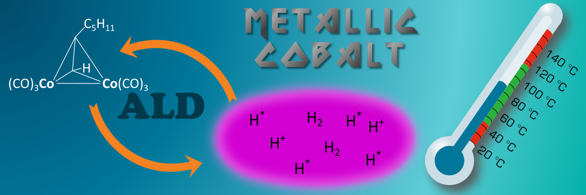
Low temperature atomic layer deposition of cobalt using dicobalt hexacarbonyl-1-heptyne as precursor

This paper presents the development of an atomic layer deposition (ALD) process for metallic cobalt. The process operates at low temperatures using dicobalt hexacarbonyl-1-heptyne [Co2(CO)6HC≡CC5H11] and hydrogen plasma at temperatures between 50 and 110 °C. X-ray photoelectron spectroscopy measurements could show that the deposited cobalt is in the metallic state and the established process shows a homogeneous coating at the wafer level.

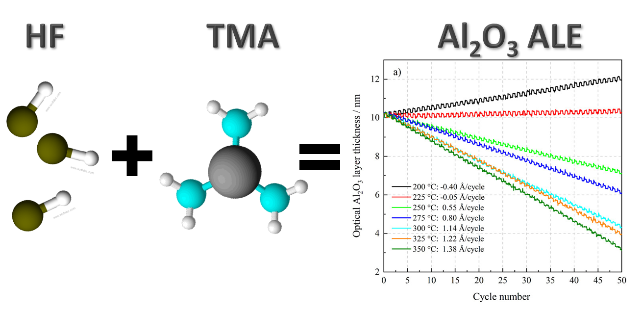
In situ studies on atomic layer etching of aluminum oxide using sequential reactions with trimethylaluminum and hydrogen fluoride

Controlled thin film etching is essential for future semiconductor devices, especially with complex high aspect ratio structures. Therefore, self-limiting atomic layer etching processes are of great interest to the semiconductor industry. In this work, a process for atomic layer etching of aluminum oxide (Al2O3) films using sequential and self-limiting thermal reactions with trimethylaluminum and hydrogen fluoride as reactants was demonstrated.

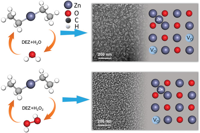
Characteristics of ALD-ZnO Thin Film Transistor Using H2O and H2O2 as Oxygen Sources

Jun Yang, Amin Bahrami, Xingwei Ding, Sebastian Lehmann, Nadine Kruse, Shiyang He, Bowen Wang, Martin Hantusch, Kornelius Nielsch ZnO thin films are deposited by atomic layer deposition (ALD) using diethylzinc as the Zn source and H2O and H2O2 as oxygen sources. The oxidant- and temperature-dependent electrical properties and growth characteristics are systematically investigated. Materials analysis … Weiterlesen

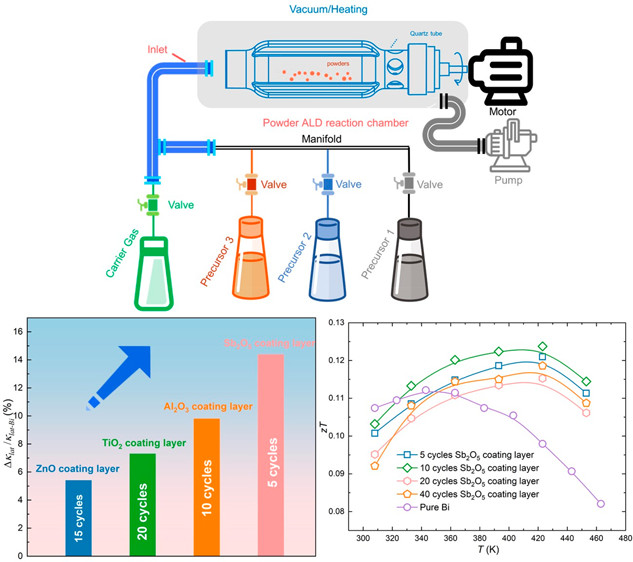
Surface Modification of Bismuth by ALD of Antimony Oxide for Suppressing Lattice Thermal Conductivity

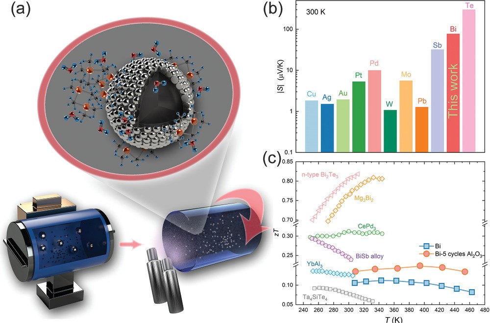
Surface modification may significantly improve the performance of thermoelectric materials by suppressing thermal conductivity. Using the powder atomic layer deposition method, the newly developed Sb2O5 thin films produced from SbCl5 and H2O2 were formed on the surfaces of Bi powders. Because of the high thermal resistance generated by Sb2O5 layers on Bi particles, a substantial decrease in κtot from 7.8 to 5.7 W m–1 K–1 was obtained with just 5 cycles of Sb2O5 layer deposition and a 16% reduction in κlat. Because of the strong phonon scattering, the maximum zT values increased by around 12% and were relocated to 423 K.

Low-Temperature Atomic Layer Deposition of High-k SbOx for Thin Film Transistors

SbOx-ALD

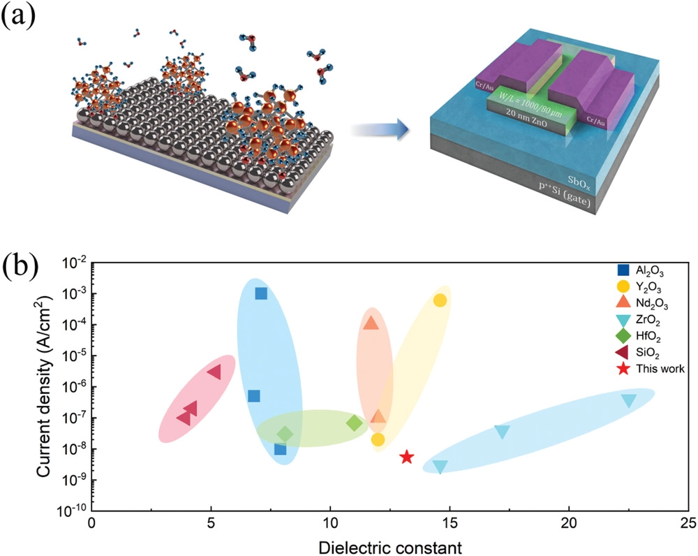
SbOx thin films are deposited by atomic layer deposition (ALD) using SbCl5 and Sb(NMe2)3 as antimony reactants and H2O and H2O2 as oxidizers at low temperatures. SbCl5 can react with both oxidizers, while no deposition is found to occur using Sb(NMe2)3 and H2O. For the first time, the reaction mechanism and dielectric properties of ALD-SbOx thin films are systematically studied, which exhibit a high breakdown field of ≈4 MV/cm and high areal capacitance ranging from 150 to 200 nF/cm², corresponding to a dielectric constant ranging from 10 to 13. The ZnO semiconductor layer is integrated into a SbOx dielectric layer, and thin film transistors (TFTs) are successfully fabricated. A TFT with a SbOx dielectric layer deposited at 200 °C from Sb(NMe2)3 and H2O2 presents excellent performance, such as a field effect mobility (µ) of 12.4 cm²/V∙s, Ion/Ioff ratio of 4∙10^8, subthreshold swing of 0.22 V/dec, and a trapping state (Ntrap) of 1.1∙10^12 1/eV∙cm². The amorphous structure and high areal capacitance of SbOx boosts the interface between the semiconductor and dielectric layer of TFT devices and provide a strong electric field for electrons to improve the device mobility.

Effect of Powder ALD Interface Modification on the Thermoelectric Performance of Bismuth

In thermoelectric materials, phase boundaries are crucial for carrier/phonon transport. Manipulation of carrier and phonon scatterings by introducing continuous interface modification has been shown to improve thermoelectric performance. In this paper, a strategy of interface modification based on powder atomic layer deposition (PALD) is introduced to accurately control and modify the phase boundary of pure bismuth. Ultrathin layers of Al2O3, TiO2, and ZnO are deposited on Bi powder by typically 1–20 cycles. All of the oxide layers significantly alter the microstructure and suppressed grain growth. These hierarchical interface modifications aid in the formation of an energy barrier by the oxide layer, resulting in a substantial increase in the Seebeck coefficient that is superior to that of most pure polycrystalline metals. Conversely, taking advantage of the strong electron and phonon scattering, an exceptionally large decrease in thermal conductivity is obtained. A maximum figure of merit, zT, of 0.15 at 393 K and an average zT of 0.14 at 300–453 K were achieved in 5 cycles of Al2O3-coated Bi. The ALD-based approach, as a practical interfacial modification technique, can be easily applied to other thermoelectric materials, which can contribute to the development of high-performance thermoelectric materials of great significance.

Current State-of-the-Art in the Interface/Surface Modification of Thermoelectric Materials

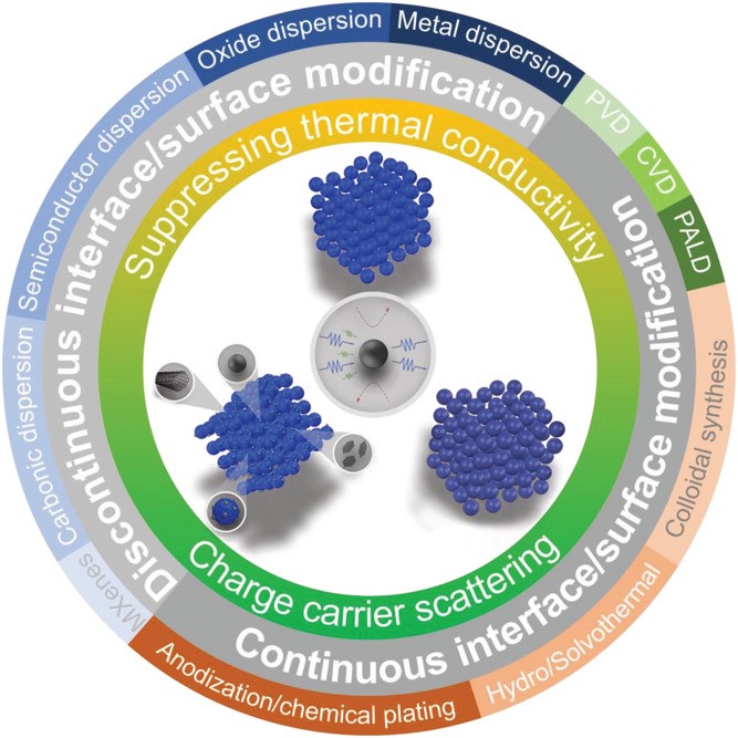
Thermoelectric (TE) materials are prominent candidates for energy converting applications due to their excellent performance and reliability. Extensive efforts for improving their efficiency in single-/multi-phase composites comprising nano/micro-scale second phases are being made. The artificial decoration of second phases into the thermoelectric matrix in multi-phase composites, which is distinguished from the second-phase precipitation occurring during the thermally equilibrated synthesis of TE materials, can effectively enhance their performance. Theoretically, the interfacial manipulation of phase boundaries can be extended to a wide range of materials. High interface densities decrease thermal conductivity when nano/micro-scale grain boundaries are obtained and certain electronic structure modifications may increase the power factor of TE materials. Based on the distribution of second phases on the interface boundaries, the strategies can be divided into discontinuous and continuous interfacial modifications. The discontinuous interfacial modifications section in this review discusses five parts chosen according to their dispersion forms, including metals, oxides, semiconductors, carbonic compounds, and MXenes. Alternatively, gas- and solution-phase process techniques are adopted for realizing continuous surface changes, like the core–shell structure. This review offers a detailed analysis of the current state-of-the-art in the field, while identifying possibilities and obstacles for improving the performance of TE materials.

Atomic layer deposition onto fabrics of carbon and silicon carbide fibers: Preparation of multilayers comprising alumina, titania-furfuryl alcohol hybrid, and titanium phosphate

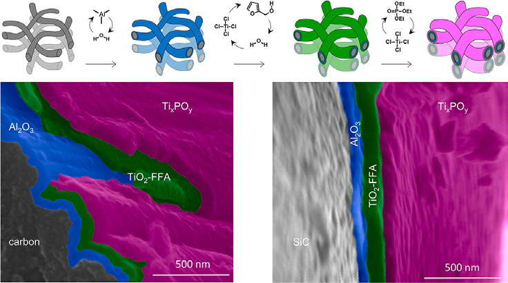
High temperature-resistant fabrics can be used as a reinforcement structure in ceramic matrix composites. They often need a coating for oxidation protection and mechanical decoupling from the matrix. Atomic layer deposition (ALD) provides very thin conformal coatings even deep down into complex or porous structures and thus might be a suitable technique for this purpose. Carbon fiber fabrics (size 300mm× 80mm) and SiC fiber fabrics (size 400mm× 80mm) were coated using ALD with a multilayer system: a first layer made of 320 cycles of alumina (Al2O3) deposition, a second layer made of 142 cycles of titania-furfuryl alcohol hybrid (TiO2-FFA), and a third layer made of 360 cycles of titanium phosphate (TixPOy).