ALPIN-Workshop 2023 – Program and Information
This year’s program and final information for the ALPIN workshop 2023 in Chemnitz.
Atomic Layer Process Innovation Network
This year’s program and final information for the ALPIN workshop 2023 in Chemnitz.
We are looking forward to contributions in the form of posters, plenary (approx. 20+5 min) or technical presentations (approx. 10+5 min) on ALD or ALE related topics.
Please register at the website and provide us with your presentation title and the type of presentation you prefer.
Der diesjährige ALPIN-Workshop wird am 11. und 12. September 2023 in der Alten Aktienspinnerei in Chemnitz stattfinden. Organisiert wird der Workshop dieses Jahr von den Kollegen am Fraunhofer ENAS und der TU Chemnitz.
Der diesjährige ALD for Industry Workshop war wie schon in den vergangenen Jahren ein voller Erfolg, dank der EFDS sehr gut organisiert und voller interessanter Vorträge, Diskussionen und Gespräche. Nachfolgend gibt es eine Auswahl an Fotos von der Veranstaltung und wer alle Fotos sehen möchte, kann dies über folgendem Link: https://www.katharinaknaut.com/index.php?seite=archiv&name=2023EFDS Am 21. und 22. … Weiterlesen
This Special Issue is dedicated to research on the development and synthesis of new compounds and their application using the atomic layer deposition (ALD) technique. In this Special Issue, original research articles and reviews are welcome.
Nur noch eine Woche bis zum diesjährigen ALPIN-Workshop – hier gibt es das Programm mit den geplanten Vorträgen. / Only one week to go until this year’s ALPIN workshop – check out the agenda with the planned talks.
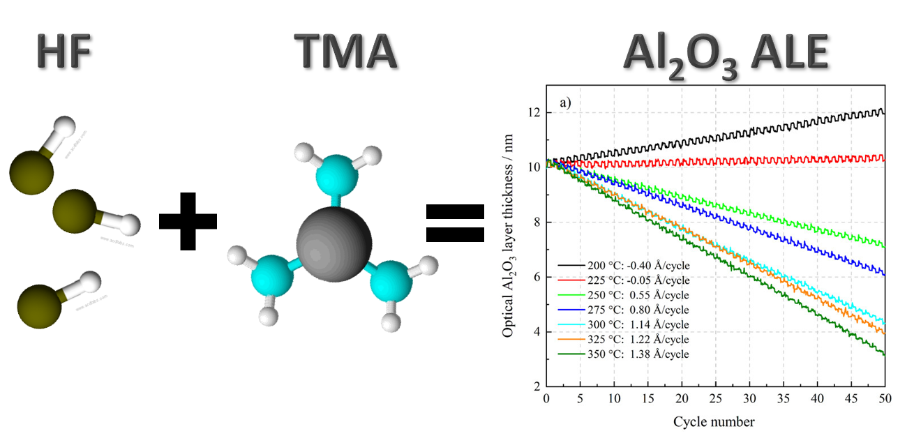
Controlled thin film etching is essential for future semiconductor devices, especially with complex high aspect ratio structures. Therefore, self-limiting atomic layer etching processes are of great interest to the semiconductor industry. In this work, a process for atomic layer etching of aluminum oxide (Al2O3) films using sequential and self-limiting thermal reactions with trimethylaluminum and hydrogen fluoride as reactants was demonstrated.
Jun Yang, Amin Bahrami, Xingwei Ding, Sebastian Lehmann, Nadine Kruse, Shiyang He, Bowen Wang, Martin Hantusch, Kornelius Nielsch ZnO thin films are deposited by atomic layer deposition (ALD) using diethylzinc as the Zn source and H2O and H2O2 as oxygen sources. The oxidant- and temperature-dependent electrical properties and growth characteristics are systematically investigated. Materials analysis … Weiterlesen
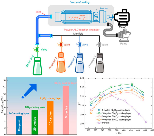
Surface modification may significantly improve the performance of thermoelectric materials by suppressing thermal conductivity. Using the powder atomic layer deposition method, the newly developed Sb2O5 thin films produced from SbCl5 and H2O2 were formed on the surfaces of Bi powders. Because of the high thermal resistance generated by Sb2O5 layers on Bi particles, a substantial decrease in κtot from 7.8 to 5.7 W m–1 K–1 was obtained with just 5 cycles of Sb2O5 layer deposition and a 16% reduction in κlat. Because of the strong phonon scattering, the maximum zT values increased by around 12% and were relocated to 423 K.
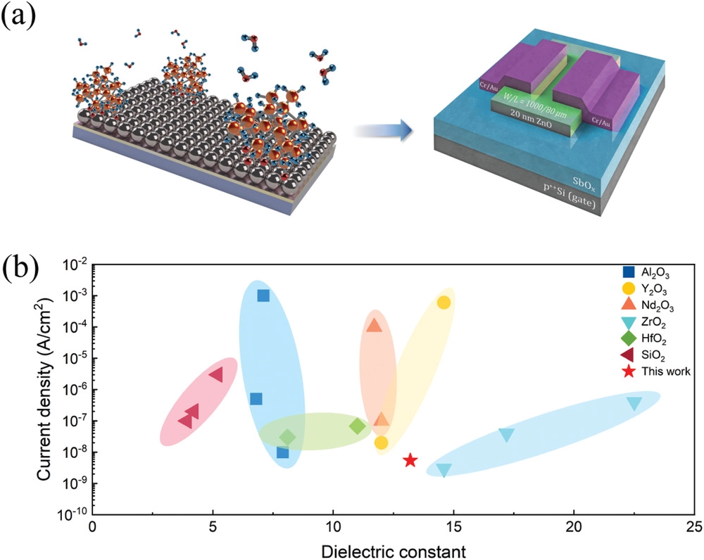
SbOx thin films are deposited by atomic layer deposition (ALD) using SbCl5 and Sb(NMe2)3 as antimony reactants and H2O and H2O2 as oxidizers at low temperatures. SbCl5 can react with both oxidizers, while no deposition is found to occur using Sb(NMe2)3 and H2O. For the first time, the reaction mechanism and dielectric properties of ALD-SbOx thin films are systematically studied, which exhibit a high breakdown field of ≈4 MV/cm and high areal capacitance ranging from 150 to 200 nF/cm², corresponding to a dielectric constant ranging from 10 to 13. The ZnO semiconductor layer is integrated into a SbOx dielectric layer, and thin film transistors (TFTs) are successfully fabricated. A TFT with a SbOx dielectric layer deposited at 200 °C from Sb(NMe2)3 and H2O2 presents excellent performance, such as a field effect mobility (µ) of 12.4 cm²/V∙s, Ion/Ioff ratio of 4∙10^8, subthreshold swing of 0.22 V/dec, and a trapping state (Ntrap) of 1.1∙10^12 1/eV∙cm². The amorphous structure and high areal capacitance of SbOx boosts the interface between the semiconductor and dielectric layer of TFT devices and provide a strong electric field for electrons to improve the device mobility.